
Scaled Printing Laboratory
The Scaled Printing Laboratory is a cutting-edge research facility enabling the fabrication of large-area printed devices such as solar cells, sensors, transistors, batteries and more. It is a research hub for screening and development of novel materials, devices, and concepts. Notably, the laboratory can also be used by external researchers and collaborators
Scaled Printing Laboratory
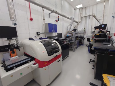
The equipment accommodated in the laboratory allows for a complete production cycle of various printed electronic devices such as organic or perovskite solar cells, organic or perovskite light emitting diodes, sensors, antennas, batteries, super capacitors, and many more. These devices can be manufactured on rigid or flexible substrates. Initial research and development activities can be undertaken on glass or plastic substrates with dimensions of up to 100 cm2. The fabrication process can then be transferred to a large-scale roll-to-roll coating process with the possibility of depositing functional materials and layers with a length of up to 100 m. It is also possible to encapsulate the fabricated devices in order to improve their stability and protect them from degradation for years. Encapsulated devices can also be tested under various ISOS degradation protocols.
The equipment in the SPL was carefully selected to allow for the complete fabrication and characterisation cycle of OE devices. Starting from the initial R&D stage on small-area surfaces, researchers can then work towards a scaled-up prototyping compatible with industry requirements and standards for large-scale fabrication on a roll-to-roll line. The similarity between the machines in the SPL and fabrication tools used in a high-volume production environment is striking and allows for an easy transfer of technology from the laboratory to the industry. To achieve a simple transfer of know-how, the following fabrication and characterisation methods and equipment were chosen:
- Laser patterning or scribing
- Slot-die-, spiral bar-, and knife coating
- Screen- and ink-jet printing
- Photonic curing
- ISOS degradation studies
Research activities
High impact research has already been taking place in the laboratory daily. Some examples are listed below:
- Inside back cover in the special issue of Small Methods “Optoelectronic Materials and Devices" Green Solvent Ethanol‐Based Inks for Industrially Applicable Deposition of High‐Quality Perovskite Films for Optoelectronic Device Applications (Small Methods 2/2024) - Rezaee - 2024 - Small Methods - Wiley Online Library
- Paper publication “Green Solvent Ethanol-Based Inks for Industrially Applicable Deposition of High-Quality Perovskite Films for Optoelectronic Device Applications”, Small Methods 2023, 2300564.
- Blog post “Perovskite solar cell upscaling prediction” by using the simulation software Laoss from Fluxim Ag and corresponding video on YouTube.
- Paper publication “A route towards the fabrication of large-scale and high-quality perovskite films for optoelectronic devices”, Sci Rep 12, 7411 (2022).
The laboratory is used daily for the fabrication of large-scale perovskite modules as part of the EPSRC funded project ‘High-Efficiency Flexible and Scalable Halide-Perovskite Solar Modules’ and for the development of large-area organic PV devices as part of the EU funded H2020 project “MUSICODE”. Some examples of deposited layers and fabricated devices are shown below:
Laser patterning or scribing
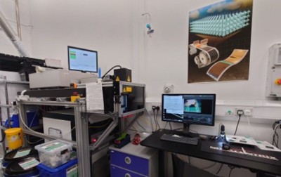
Lasers are core components of many production environments nowadays. This is due to the availability of various types of lasers, which operate at different wavelengths and allow for a reliable and high-accuracy use depending on the scope of application.
The laser in the SPL was selected for one main purpose: the precise patterning of functional layers in OE devices, where organic, inorganic, or semi-conducting materials are used. We chose a pico-second HyperRapid NX laser from Coherent, which operates at 532 nm and has a maximum power of 50 W. This is a high-end laser used in industry for micro-machining and allows the users of the SPL to selectively remove functional layers with an accuracy of app. 15 µm with high speed and reliability. With this laser it is possible to carry out the P1-P2-P3 patterning process used in the solar cell industry.
There is a second laser housed within the labs of the ATI. It is a Nd:YAG laser with 4 emission wavelengths: 266nm, 355nm, 532 nm and 1064 nm. This tool is dedicated for time-of-flight and Current Extraction by Linearly Increasing Voltage (CELIV) characterisation of organic semiconductors.
Coating techniques
Different coating techniques, such as slot-die-, knife-, or spray coating can be used for the fabrication of large-area printed electronics. These can be employed on rigid substrates (such as glass) or on flexible alternatives (such as plastics or flexible glass). Working on rigid substrates usually means that a sheet-to-sheet (S2S) production will be used. Although large-areas are possible for the S2S process, the fabrication takes place in a “stop-and-go” manner which limits the production speed. In contrast, a roll-to-roll (R2R) process allows for high production speeds and, therefore, higher number of production units. In the SPL we can do both.
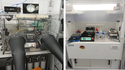
- S2S Deposition
There are two S2S capable coaters in the SPL. One of our coaters is located in a glove box which can operate with different inert gases. The second coater is placed in an extraction fume hood and works in air. Both coaters allow for the deposition of functional inks by means of using one of the following coating techniques: slot-die-, spiral bar-, or knife coating. Both flexible and rigid substrates with maximum dimensions of 10 cm x 10 cm can be used and the operator can adjust various coating parameters such as coating speed and gap, temperature of the stage, deposition rate.
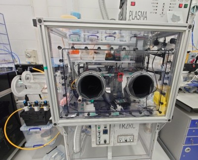
- R2R Deposition
After the successful development and fabrication of functional devices using the S2S coaters, the fabrication process can be upscaled to a pilot line. This can be accomplished with the R2R coater in the SPL, which can be used for slot-die and spray coating of functional materials. Similar to the S2S process, the operator can adjust various coating parameters and choose the drying conditions after the coating: UV, IR, hot gas, and a combination of the above.
Printing Techniques
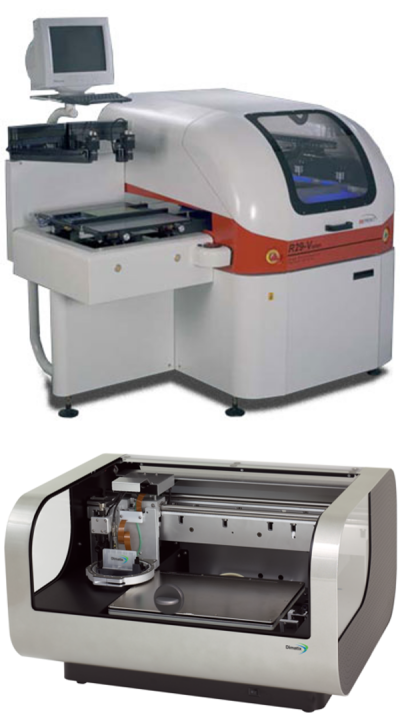
- Screen printing
During the screen printing process, a desired pattern is created by pressing ink with a squeegee through a stencil (also known as screen). The screen printing can be accomplished in a S2S or a R2R process allowing for high throughput fabrication.
The screen printer in the SPL is capable of printing on areas up to 50 cm x 50 cm. It can deposit various metal-, organic-, semi-conducting-, dielectric-, or carbon-based inks. The equipment can be used for the fabrication of sensors, el. circuits, RFIDs, antennas, or top electrodes for solar cells and OLEDs.
- Ink-jet printing
Similar to the screen printing, ink-jet printing can be used in an S2S or R2R production environment. It allows for the precise ejection of ink droplets in order to create a high resolution pattern on a substrate. Equivalently to the screen printer, the ink-jet printer in the SPL can be used for the deposition of various inks.
Photonic curing
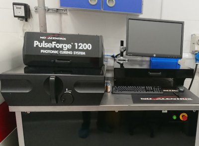
Photonic curing is the high-temperature thermal processing of a thin film using pulsed light from a flashlamp. When this transient processing is done on a low-temperature substrate such as plastic or paper, it is possible to attain a significantly higher temperature than the substrate can ordinarily withstand under an equilibrium heating source such as an oven.
Considering the advantages of photonic curing compared with conventional heat treatments, the system in the SLP allows for the drying and sintering of various inks, such as metal nano-particles- or carbon-based inks.


