Quantum technology with deterministic ion implantation
We develop new strategies to produce quantum qubits, sensors and emitters using defects in solids using Surrey’s National Ion Beam Centre - Controlling and characterising their properties through use of Free Electron Lasers, high magnetic fields and synchrotrons.
Overview
We have a vibrant experimental programme focused on research with ion beams, which provide the only quantum-technology fabrication methodology that seamlessly integrates with existing microelectronic processes and allows for large-scale production involving the incorporation of single impurity qubits via implantation. This technique promises qubit arrays large enough for error correction and the potential for mass production of identical devices. Fully developed deterministic single-ion implantation is crucial to exploit the full potential of impurity-based quantum technologies for scale-up.
Implantation of single qubit atoms in silicon presents a viable solution. However, current research primarily focuses on the stochastic incorporation of impurities, with only limited control over placement using masks or focused beams. Defect complexes in diamond have shown early success in quantum computing by demonstrating qubits at room temperature. Presently, ISI is not utilised for nitrogen-vacancy (NV) centres in diamond, as nitrogen is a naturally occurring impurity in diamond, and implantation tends to produce vacancies that combine with pre-existing nitrogen atoms.
Deterministic ISI can generate defect complexes in silicon carbide, where photonic devices for quantum networks have already been demonstrated using focused ion beams, albeit without precise control over the number of implanted ions. This technology could also be expanded to include rare-earth impurities for quantum communications with further ion-source development. While it is feasible to locate a random defect complex and then construct device architecture around it, a deterministic approach to producing colour centres would significantly enhance commercial manufacturing yields.
Research Team:
For relevant publications in this research area, please consult the websites of the research team members above.
Funding:
The SIMPLE tool for implanted single ions

The Ion Beam Centre, an EPSRC National Research Facility, houses the SIMPLE tools (for Single Ion Mult-Species Positioning at Low Energy https://uknibc.co.uk/SIBC/QImplant.php). The tool was made by our collaborators at Ionoptika Ltd, and the tools can implant single, deterministic impurities with few-nanometer lateral precision. The number of atomic species we can implant is rising steadily, as is the accuracy with which we can perform the implantation.
We are exploring the possibilities of using ion implantation to create single photon sources (SPS) which are crucial for secure communications and advanced quantum computing systems. These can be formed by the implantation of impurities such as rare earth erbium, or the creation of defect centres.
At the same time we are working to improve the positioning accuracy. This research applies lateral solid-phase epitaxial regrowth to improve the placement of impurities in semiconductors. Our methodical approach aims to refine single ion implantation accuracy, potentially advancing quantum computing applications by ensuring precise impurity positioning.
Physics of solid-state impurities and defects

The impurities and defects in solids provide a well-known spin-qubit platform. We have been primarily studying the states of silicon (and germanium) donors. The internal transitions between the orbital states of donors lie in the far-infrared (THz) region of the electromagnetic spectrum, requiring specialised sources for their control. Surrey is the leading group in the UK for THz spectroscopy of picosecond-scale dynamics in semiconductors, through its use of the free-electron-laser facility FELIX in Nijmegen.
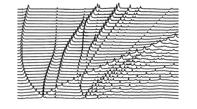
We also use the high magnetic-field facility in Nijmegen (HFML). By utilising magnetic fields as a non-invasive tool, we can intricately modify the energy states within electronic materials. This technique allows precise control of electron motion, facilitating identification of key properties — for instance, tuning the energy levels of silicon donors to resonate with specific phonon modes, shedding light on donor relaxation mechanisms. Understanding these interactions may lead to strategies for enhancing quantum-state lifetimes, improving the efficiency of quantum-computing elements.
Our research has achieved near-perfect efficiency in detecting single-ion implantation events within silicon-on-insulator (SOI) devices — a breakthrough critical for investigating spatial precision of single-ion implants using focused-ion-beam systems, laying the groundwork for scalable production of solid-state quantum computers.
Nanofabrication with ion beams

Our research introduces a refined process using ion beam irradiation to precisely engineer strain in single-crystal silicon membranes by controlling the degree of amorphisation around the active crystal. This is akin to tightening the skin of a microscopic drum by treating the edges.
This method offers significant potential for advancing photonics and quantum technologies, enabling enhanced performance in germanium-based optoelectronics and precise manipulation of material quantum properties via strain introduction/ cancelling without creating spin impurities in the device region.


