Breakthrough in carbon nanotube patterning
ACS: Applied Materials and Interfaces has published research by the University of Surrey’s Dr Simon King that reports on a faster and more energy efficient method of patterning carbon nanotubes for specific devices.
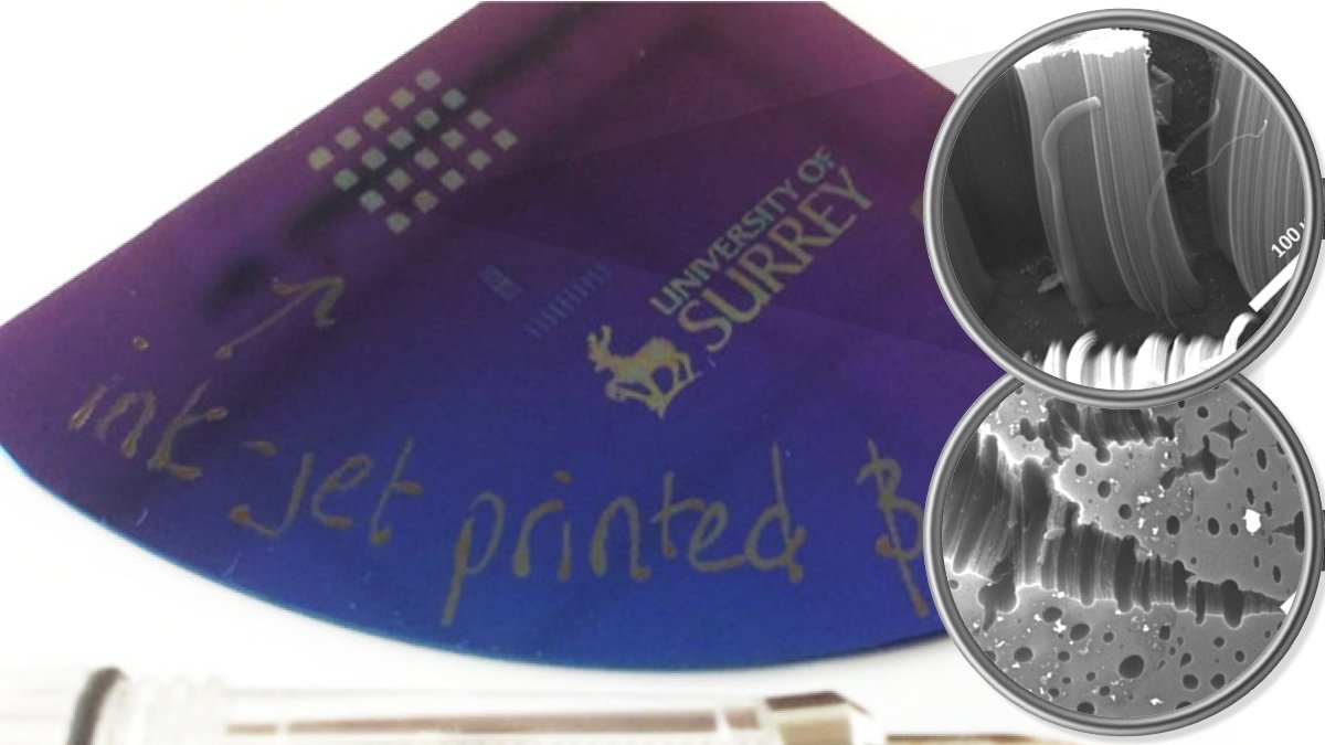
Dr King has found a way to precisely pattern and 'grow' microscopic CNTs (right) via inkjet printing
“Carbon nanotubes, or CNTs as they’re known, are very small cylindrical graphitic carbon structures, which are now seeing use in metal-free, lightweight and flexible electrical devices,” says Dr King, who’s a Research Fellow at Surrey’s Advanced Technology Institute (ATI). “But the problem CNTs have is they need to go through quite energy-intensive and time-consuming processes to pattern them and make them usable for specific applications.
“For example, in conventional copper electronics you print a circuit on an underlying layer called a substrate. However, with CNTs you’d normally need a catalyst precursor, which is the seed material the CNTs ‘grow’ from. Patterning the catalyst typically needs a number of prolonged steps in order to form the CNTs into shapes to make them usable for specific devices; making commercial manufacturing expensive.”
Thanks to research conducted by Dr King, building on research previously conducted by Dr Liam McCafferty, these additional post-processing techniques may soon be redundant.
“What we’ve done is make a multi-purpose precursor solution that can be used to ‘grow’ CNTs directly in place, in any pattern, for any device,” continues Dr King. “In the paper we’ve just published in ACS: Applied Materials and Interfaces, we demonstrate the solution using inkjet printing, spray painting, stamping and handwriting.
“So, instead of companies being forced to pattern CNTs using the conventional slow and energy-intensive methods, they can now use this novel precursor as an ink, and inkjet print the solution to precisely grow CNT structures for devices on a commercial scale.”
This breakthrough could have long-term impact in a number of large-scale manufacturing industries.
Dr King adds: “Organic electronics will probably be the area of its biggest application because everyone’s moving away from metal in manufacturing electrical devices. For example, in computing we use interconnects, which are tiny metal pins on the back of processing chips. So how we make these can change.
“We also live on a carbon-rich planet, so if we swap the use of mined metals in electronics for using CNTs, the impact could be huge.
“To summarise, using our universal precursor means you can manufacture faster, it’s less energy intensive and it's moving away from metals into carbons.”
Professor Ravi Silva, Director of Surrey’s Advanced Technology Institute, said: ”The work presented by Simon in this paper is underlined by over two decades of research in nanocarbon materials.
“It will open a whole new area in wearable and future Internet-of-Things-type technologies that need new solutions for unique problems.”
Find out more on the Advanced Technology Institute and its research.

