
Nanomaterials and nanocomposites
Read about our nanomaterials and nanocomposites research.
What are composite materials?
An example of nanocomposites is the aerospace industry where composite usage has risen from one/two percent in the 1970s to 50 percent in 2010. Other industries that are incorporating composites include the automobile, marine, construction, biomedical and sporting equipment.
Composite materials are typically composed of multiple materials that complement each other. For instance, strong and stiff carbon fibres that are protected by a plastic which encapsulates the fibres and allows load or force to be effectively distributed amongst them.
So what is preventing complete adoption of composite materials? And where can the development take us? We believe nanotechnology can play a pivotal role in answering these questions.
Research areas

Copper interconnects, when miniaturised, suffer from poor conductivity and electromigration, where the interconnect can thin at high current loads. This is why extracting heat from computer microprocessors is crucial, and new materials and solutions are required to cope with the increased miniaturisation and demand for power. High-quality carbon nanotubes have high current carrying capabilities, high thermal conductivity and high tensile strength and are ideal replacements, provided they can be produced and manipulated at conditions compatible with semiconductor processes.
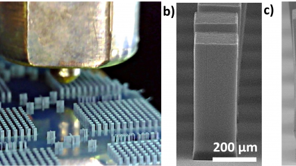
Vertically-aligned carbon nanotubes (VACNTs) grown with conventional chemical vapour deposition methods at low temperatures (below 600oC), result in highly defective, low density VACNTs with low growth rates, which is unsuitable for both industrial feasibility and interconnect applications. The Graphene Centre at the ATI can grow patterned, high-aspect ratio, high-quality CNT whilst maintaining the substrate temperature below 450°C (Figure 1).
These interconnects have very good mechanical properties, with excellent compliance and electrical contact reproducibility, however a well-designed metal capping contact is required to ensure an ohmic-type contact.
Selected publications
GOPEE, V., THOMAS, O., HUNT, C., STOLOJAN, V., ALLAM, J. & SILVA, S. R. P. 2016. Carbon Nanotube Interconnects Realized through Functionalization and Sintered Silver Attachment. Acs Applied Materials & Interfaces, 8, 5563-5570.
TAS, M. O., BAKER, M. A., MASTEGHIN, M. G., BENTZ, J., BOXSHAL, K. & STOLOJAN, V. 2019a. Highly Stretchable, Directionally Oriented Carbon Nanotube/PDMS Conductive Films with Enhanced Sensitivity as Wearable Strain Sensors. Acs Applied Materials & Interfaces, 11, 39560-39573.
TAS, M. O., BAKER, M. A., MUSARAMTHOTA, V., UPPAL, H., MASTEGHIN, M. G., BENTZ, J., BOXSHALL, K. & STOLOJAN, V. 2019b. Carbon nanotube micro-contactors on ohmic substrates for on-chip microelectromechanical probing applications at wafer level. Carbon, 150, 117-127.
Spider-Man's secret weapon! This manufacturing technique allows us to form very thin, spider-web-like fibres (ranging from ~50 nanometres to a few microns) by pulling very thin strings out of a droplet of polymer, under a high voltage (~10-60 kV).
Nanomaterials in the polymer can align as the polymer fibre stretches and dries, and the whole material can be collected on a drum, a flat sheet or even a textile fabric for applications in energy harvesting, tissue engineering, composites, electrical shielding and electrical conductivity applications. Electrospun mats are widely used for filtration, energy storage and are the base ingredient of ultralight sponges.
This way we can harness the possibilities opened by nanomaterials on the large scale; for example, aligning carbon nanotubes, removing the polymer and finding a way to connect the nanotubes with strong sp2-bonds can lead to electrical cables that are as conductive as copper, but up to seven times lighter.
Currently we are investigating many applications, including:
- Carbon nanotube (CNT) wire & yarn spinning, as a lightweight highly conductive alternative to copper wires and organic antennas
- Nanofibre composites and composite reinforcements, for next generation lightweight enhanced composite materials (magnetic CNT composite pictured below)
- Large area nanomaterial alignment, for industrially viable roll to roll fabrication of nanomaterial devices
- High output triboelectric textiles, for personal power generation
- Supercapacitor electrodes and dielectric separators
- Nanofibre biological scaffolds
- Electrochemical biological sensors.
Featured papers
S.G. King, L. McCafferty, V. Stolojan, S.R.P. Silva, Highly aligned arrays of super resilient carbon nanotubes by steam purification, Carbon N. Y. 84 (2015) 130–137. doi:10.1016/j.carbon.2014.11.061.
Simon G. King, Vlad Stolojan, S. Ravi P. Silva, Large area uniform electrospun polymer nano-fibres by balancing of the electrostatic field, Reactive and Functional Polymers, 2017, doi.org:10.1016/j.reactfunctpolym.2017.10.017.
Materials with physical dimensions reduced to the nanoscale (less than 100 nm) can exhibit markedly different properties compared to those on larger length-scales.
This is mainly a result of the massively increased fraction of atoms that are at the surface of the material or the confinement of charge carriers on length scales similar to their quantum mechanical wavelength.
Much of the interest in nanotechnology stems from these unique quantum and surface phenomena that matter exhibits at the nanoscale. As the majority of the atoms in these nanostructures are a short distance from the surface, the optical and electrical properties of these systems can be strongly modified by changes in their environment, allowing a host of applications particularly in sensing.
In recent years the techniques for growing and fabricating nanoscale materials have matured significantly, to the point where researchers are able to tailor their properties toward particular applications, allowing the production of truly functional nanomaterials, which utilise these properties and allow the fabrication range of new and exciting technologies.
What we are doing
We are investigating many different functional nanomaterials, such as:
- Metal nanoparticles
- Metal oxide nanowires
- Carbon nanotubes for a range of applications including:
- Physical, chemical and environmental sensors
- Energy scavenging materials
- Low-cost transparent conductors
- Optoelectronic devices.
We have recently demonstrated a laser writing technique to produce miniature vapour nanosensors, based around metal nanoparticles, on low cost substrates. The processing conditions are in ambient air and the devices, including all electrodes, were fabricated in one step. Sensors based on palladium metal nanoparticles where fabricated and tested and shown to be able to detect hydrogen, and gold nanoparticle sensors were fabricated to detect relative humidity.
Featured paper
M. J. Beliatis, N. A. Martin, E. J. Leming, S. R. P. Silva, and S. J. Henley, “Laser Ablation Direct Writing of Metal Nanoparticles for Hydrogen and Humidity Sensors”, Langmuir, 27, 1241 (2011).

Our experience in nanomaterial fabrication, manipulation and analysis has enabled us to make significant progress in addressing a current issue in the aerospace industry: How to remove the dependence of metallic structures which are employed to give lightning strike protection as composites have poor electrical conductivity.
Achieving this would reduce weight further and avoid manufacturing difficulties in incorporating metals with composites.
The method
Our method was to use carbon nanotubes – hexagonal array of carbon atoms (graphene), rolled into tubes. These carbon nanotubes are very small, with a thickness measuring around 1/5000th of a human hair (roughly speaking, 5000 carbon nanotubes stacked in a line would equal a human hair). Nonetheless, they have exceptional mechanical, electrical and thermal properties.
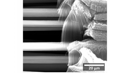
These carbon nanotubes are grown directly on the carbon fibres at a very high density, in fact 10 billion per cm2, substantially increasing the surface area of the carbon fibre and increasing the ability of the carbon fibres to ‘hold on to’ the plastic, improving key mechanical properties. Crucially, however, the carbon nanotubes bridge from carbon fibre-to-carbon fibre (see image below) imparting electrical and thermal conductivities.
Exciting possibilities
Furthermore, the technology will lead to exciting possibilities such as energy harvesting within storage structures and sensory technology with self-healing capabilities. Therefore, we expect structures to combine additional functionality.
For instance, a plane, where the vibrations and motions made by the wing are utilised in generating and storing electrical power and any damage occurred can be detected and repaired - in flight!
Nanocomposite materials combine the beneficial properties of two or more separate constituents to create unique and innovative new materials for a plethora of applications, from energy storage to targeted cancer treatment, aerospace coatings to catalysts.
We decorated carbon nanotubes with iron nanoparticles to create magnetic composite materials. These materials were shown to reversibly absorb organic dyes which provides a basis for applications in wastewater purification and oil spill recovery. Where the contaminant (oil or dye) is adsorbed by the material, which is subsequently removed with a magnet before the contaminant is removed and the material reused.
The robust attachment of the iron nanoparticles to the carbon supports are demonstrated with resistance to acid dissolution also being shown through a protective carbon coating. The nanocomposite can be mixed with a polymer and electrospun into aligned nanocomposite fibres to produce a soft magnetic composite with future applications in sensors and fast switching solenoids.
Featured article
L. McCafferty, V. Stolojan, S.G. King, W. Zhang, S. Haq, S.R.P. Silva. Decoration of Multiwalled Carbon Nanotubes with Protected Iron Nanoparticles. Carbon 2015; 84, 47-55. doi:10.1016/j.carbon.2014.11.042.

Collaborate with us
If you'd like to find out more about functional nanomaterials then take a look at the Functional Nanomaterials Group who focus on micro-scale processing, materials integration and manufacture to allow the creation of unique 3D micro- and nano-scale structures.